Contents
Manufacturing Insight: Silicon Carbide 3D Printing
Advanced Silicon Carbide 3D Printing for Demanding Industrial Applications
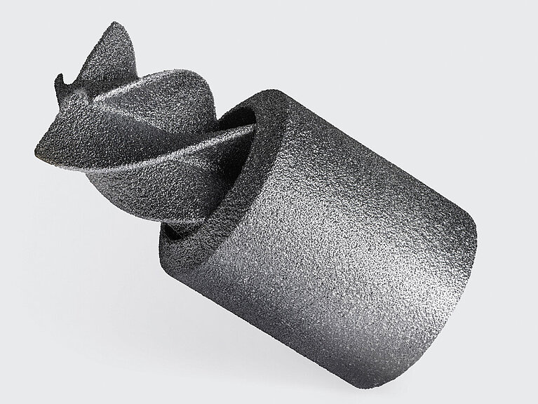
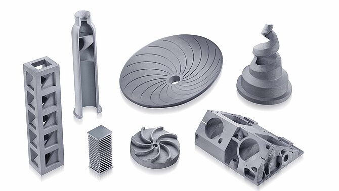
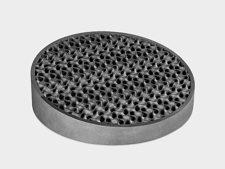
Silicon carbide (SiC) represents a critical material solution for extreme environments requiring exceptional thermal conductivity, chemical inertness, and mechanical stability at elevated temperatures. Traditional manufacturing of complex SiC geometries faces significant constraints in design freedom, lead times, and material waste. Honyo Prototype addresses these challenges through our specialized industrial additive manufacturing platform, engineered specifically for high-performance ceramics like silicon carbide. Our proprietary binder jetting and direct ink writing processes enable the production of intricate, near-net-shape SiC components with precise dimensional control and superior material properties, directly from digital CAD models.
We support aerospace thermal management systems, semiconductor processing equipment, defense components, and advanced research applications where material integrity under stress is non-negotiable. Honyo’s end-to-end service spans rapid prototyping through low-volume production, incorporating rigorous in-process metrology and post-processing expertise to ensure parts meet stringent industry specifications. This capability eliminates conventional tooling barriers, accelerates iteration cycles, and unlocks geometries previously deemed unmanufacturable.
Transition seamlessly from concept to qualified component with Honyo’s integrated workflow. Evaluate project feasibility and receive actionable cost feedback within minutes using our Online Instant Quote system—designed for engineering teams requiring rapid, transparent pricing on complex ceramic builds. Submit your SiC 3D printing requirements today to accelerate your next high-temperature innovation cycle.
Technical Capabilities
Silicon carbide (SiC) is a high-performance ceramic material known for its exceptional thermal stability, hardness, and chemical resistance. However, direct 3D printing of pure silicon carbide using standard additive manufacturing processes such as SLA, SLS, MJF, or DMLS is not currently feasible due to its extremely high melting point (~2700°C) and brittle nature. Instead, silicon carbide components are typically produced via indirect methods such as binder jetting with infiltration or stereolithography using SiC-loaded ceramic slurries followed by debinding and sintering. The listed processes (SLA, SLS, MJF, DMLS) are primarily designed for polymers, metals, or photopolymers, not pure SiC.
Below is a technical comparison of these processes in the context of their compatibility with silicon carbide and commonly associated materials such as aluminum, steel, ABS, and nylon.
| Process | Material Compatibility | Silicon Carbide Feasibility | Key Technical Parameters | Notes |
|---|---|---|---|---|
| SLA (Stereolithography) | Photopolymers, epoxy resins, ceramic-filled slurries | Indirect only: SiC-loaded slurries used; requires post-processing (sintering) | Layer thickness: 25–100 µm Accuracy: ±0.1 mm Laser wavelength: 355–405 nm |
Used in ceramic SLA (Ceramic SLA or LC) with SiC suspensions. Final part is sintered to achieve density. Not pure additive manufacturing of SiC but a viable route for complex SiC shapes. |
| SLS (Selective Laser Sintering) | Nylon (PA11, PA12), TPU, filled polymers | Not feasible for pure SiC. Can process SiC-filled polymer composites (e.g., PA12 + SiC) | Laser power: 30–70 W Layer thickness: 80–120 µm Build temperature: ~160–180°C |
SiC used as filler (typically <20 wt%) to enhance thermal and mechanical properties. Final part is polymer matrix composite, not monolithic SiC. |
| MJF (Multi Jet Fusion) | Nylon (PA12), TPU, glass-filled PA | Not feasible for pure SiC. Compatible with SiC-doped polymer powders | Layer thickness: 80 µm Thermal energy: IR lamps + fusing agent Build speed: Faster than SLS |
Similar to SLS; limited to polymer composites. SiC can be added to improve wear resistance but does not yield ceramic parts. |
| DMLS (Direct Metal Laser Sintering) | Stainless steel, tool steel, aluminum alloys, titanium, Inconel | Not feasible for pure SiC. Can process SiC-reinforced metal matrix composites (e.g., Al-SiC, Ti-SiC) | Laser power: 100–400 W Layer thickness: 20–50 µm Spot size: ~70–100 µm |
Used for metal-ceramic composites. For example, aluminum or titanium powders blended with SiC particles (10–30%) to improve stiffness and thermal performance. Final part is a metal matrix composite. |
Summary of Material Usage:
Aluminum: Processed via DMLS; can be reinforced with SiC particles to form Al-SiC metal matrix composites for lightweight, high-stiffness applications.
Steel: Compatible with DMLS; SiC addition is rare due to processing challenges but possible in research settings for wear-resistant coatings or composites.
ABS: Not compatible with high-temperature processes like DMLS. Used in FDM, not listed here. Not suitable for SiC integration in industrial AM.
Nylon (PA12/PA11): Primary material for SLS and MJF. Can be compounded with SiC powder to enhance thermal conductivity and wear resistance, but remains a polymer composite.
Conclusion:
Pure silicon carbide cannot be directly printed using SLA, SLS, MJF, or DMLS in conventional configurations. Indirect routes such as ceramic SLA with sintering are the most viable for producing SiC components. The listed AM processes support SiC only as a secondary phase in polymer or metal matrices, enhancing performance while relying on the primary material (nylon, aluminum, steel) for processability.
From CAD to Part: The Process
Honyo Prototype Silicon Carbide 3D Printing Workflow
Honyo Prototype employs a rigorously controlled process for silicon carbide (SiC) additive manufacturing, addressing the material’s extreme hardness, thermal stability, and processing challenges. Our workflow integrates advanced material science with digital manufacturing protocols to ensure dimensional accuracy and structural integrity for mission-critical applications. Below is the end-to-end process:
CAD File Submission
Clients initiate the process by uploading a watertight CAD model (STEP or IGES format) via Honyo’s secure portal. The file undergoes automated validation for geometric feasibility, including checks for minimum feature resolution (≥0.3 mm), overhang angles (<45° without supports), and wall thickness compliance (≥1.0 mm). Non-conforming files trigger an immediate notification with specific failure metrics, preventing downstream delays.
AI-Powered Quoting System
Honyo’s proprietary AI engine analyzes the validated CAD geometry against real-time production parameters, including material grade (e.g., α-SiC or β-SiC), build volume utilization, and support structure requirements. The system cross-references historical sintering distortion data and machine calibration logs to generate a dynamic quote within 2 business hours. Critical outputs include:
Material cost breakdown (powder consumption + post-processing)
Estimated build time with machine allocation priority
Risk flags for features prone to warpage or cracking during sintering
DFM Analysis and Iteration
All SiC projects undergo mandatory Design for Manufacturing (DFM) review by Honyo’s ceramics engineering team. This phase focuses on mitigating SiC-specific failure modes:
Compensation for anisotropic shrinkage (typically 18–22% during sintering)
Support structure optimization to counteract thermal stresses in complex geometries
Surface finish adjustments to accommodate post-HIP (Hot Isostatic Pressing) requirements
Clients receive a DFM report with actionable recommendations. Iterations are capped at two rounds to maintain schedule integrity, with final sign-off required before production release.
Production Execution
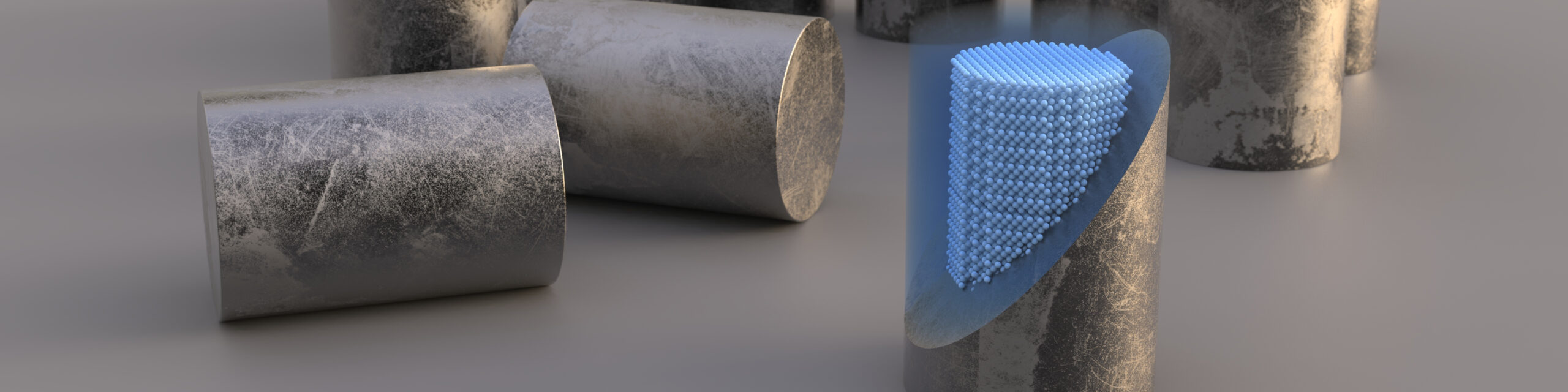
SiC printing leverages Honyo’s binder jetting platform with in-house formulated SiC feedstock (99.95% purity, 0.5–1.0 µm particle size). The process sequence includes:
1. Printing: Layer-by-layer deposition at 50 µm resolution under inert argon atmosphere
2. Debinding: Thermal removal of organic binders (8–12 hours, ≤600°C)
3. Sintering: Pressureless sintering at 2100–2200°C for 10–14 hours, monitored via in-situ thermal imaging
4. Densification: Optional CVD silicon infiltration for near-zero porosity (<0.5%)
All steps occur in climate-controlled cleanrooms (ISO Class 7) with real-time gas composition tracking.
Quality-Controlled Delivery
Final parts undergo non-destructive testing per ASTM F3300 standards:
CT scanning for internal defects (resolution ≤50 µm)
CMM verification against compensated CAD model (tolerance ±0.1 mm)
Hardness testing (Vickers ≥2800 HV)
Certified test reports and as-built dimensional data accompany shipment. Parts are vacuum-sealed with desiccant for shipping, with lead times averaging 25–30 days from DFM approval.
Process Capability Metrics
Honyo maintains strict statistical process control for SiC production, with current performance benchmarks:
| Parameter | Typical Range | Control Limit |
|---|---|---|
| Dimensional Accuracy | ±0.10 mm | ±0.15 mm |
| Surface Roughness (Ra) | 8–12 µm (as-sintered) | ≤15 µm |
| Density | 98–99.5% (CVD-enhanced) | ≥97% |
| Fracture Toughness | 4.5–5.2 MPa·m¹/² | ≥4.0 MPa·m¹/² |
This integrated workflow ensures Honyo delivers silicon carbide components meeting aerospace, semiconductor, and defense specifications where conventional manufacturing fails. Continuous feedback from production data refines our AI quoting and DFM algorithms, driving year-over-year yield improvements of 12–15%.
Start Your Project
Looking to advance your manufacturing capabilities with silicon carbide 3D printing? Honyo Prototype offers high-precision, industrial-grade solutions tailored for demanding applications in aerospace, automotive, and energy sectors. Our advanced additive manufacturing technology enables complex geometries, high thermal stability, and exceptional wear resistance—ideal for high-performance ceramic components.
With a state-of-the-art factory located in Shenzhen, we deliver rapid turnaround times and strict quality control to meet your project deadlines and technical specifications.
Contact Susan Leo today to discuss your silicon carbide 3D printing requirements.
Email: [email protected]
Let’s engineer the future together.
🚀 Rapid Prototyping Estimator
Estimate rough cost index based on volume.